 3D Microelectronics
 3D Microelectronics
![]()
This document provides a summary of the activities undertaken on an ONR funded program at Northeastern University and Kopin Corporation to develop three dimensional microelectronics. As a demonstration vehicle we have chosen a 64 bit RISC microprocessor. Two interim goals are sought; a test chip to demonstrate the three dimensional technology capability with ring oscillators and gate delay chains. This chip is expected to be completed this year. Our second objective is a 32 bit RISC microprocessor. To achieve this goal, new design tools are needed. These are near completion and described within this document.
I) Introduction
Recent advances in integrated circuit technology have focused on reducing device sizes and increasing device speeds. As a result of these developments, circuit designers are able to boost the performance of their designs by 25% annually. While circuit speeds are increasing, the desire for increase functionality has resulted in increased die size. Interconnections between functional blocks require long lead lengths. This leads to a reduction in overall circuit speed. Our approach to increasing circuit speed while at the same time maintaining die size and increasing functionality is the utilization of three-dimensional (3-D) microelectronics. In this approach, multiple layers of devices are stacked on top of each other with insulating material between them. The advantages of the 3-D electronics approach are that:
The main objectives of the program are provided below.
Our technology takes advantage of the Transferred Circuits (TC) capabilities
that have been developed by Kopin Corporation. Using the TC technique,
circuits can be fabricated using standard bulk CMOS processing and then
transferred from one wafer to another in thin film form. The transfer process
allows alignment of the layers. At Northeastern, we are developing an interconnection
technology that will allow layers to be electrically connected to one another.
These interconnections are small and can be placed anywhere on the die.
This unrestricted placement of interconnections gives our technology a
unique advantage over other existing 3D techniques.
Our current work is aimed at the development of a two level circuit. In this case, a bulk silicon wafer is processed with half of the circuit. A second Silicon-on-Insulator (SOI) wafer is processed using standard CMOS fabrication techniques creating the second half of the circuit. The second wafer is manufactured on Isolated Silicon Epitaxy (ISE), Kopin Corporation's production Silicon-On-Insulator (SOI) technology. SOI consists of a bulk silicon substrate with a thin layer of single crystalline silicon on top and separated from the substrate by a silicon dioxide layer. The SOI wafer is used because the buried oxide layer acts as a etch-stop during a subsequent back-etch step. The SOI circuit will be transferred face down onto the top of the bulk wafer as shown in Figure 1.
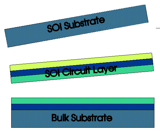
Figure 1. Transfer process taking the device layer from the SOI wafer and bonding it to the top of a processed bulk silicon wafer.
An adhesive is used to bond the transferred circuit to the bulk silicon wafer. The result is the two layer 3-D circuit shown in Figure 2.
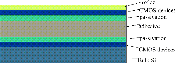
Figure 2. A simplified cross-sectional view of a 3-D circuit created using Kopin's circuit transfer technology.
Electrical connections need to be made between the two active device layers after the transfer. A major task in our 3-D program is the development of a process to make the electrical interconnection. A conceptual drawing of an interconnection is shown in figure 3 below. During the program, interconnection test structures have been fabricated and tested. Interconnections with vias as small as 10 microns square have been produce good results.

Figure 3. A cross-sectional view of a complete 3D circuit showing a bulk device, an SOI device and an interconnection.
The transfer technique has the following advantages over other 3D methods:

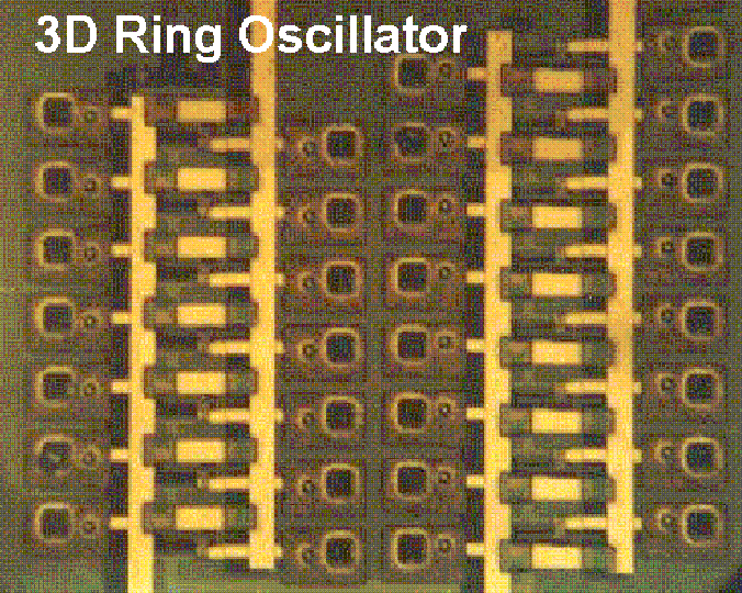
Figure 4. Optical micrograph of a 3D ring oscillator showing SOI and bulk inverters and interconnections ( dark paired large and small regions). The SOI inverters are each connected to bulk inverters so that the ring oscillator threads up and down through the 3D structure. This device was meant to demonstrate the feasibility of the interconnection scheme.
To exploit the capabilities of our 3-D process, we will develop two
microprocessor designs. The motivation behind choosing a design as intricate
as a microprocessor is two-fold. First, we need a design in which we will
extensively exercise our customized 3-D design tools. Second, the layout
and routing of a microprocessor is a difficult task in itself, and thus
we can fully exploit the routing and layout advantages provided by 3-D
technology. To be able to design and fabricate a microprocessor, we needed
to develop a design platform which would support 3-D VLSI design.
We have developed or enhanced a number of VLSI
CAD tools to aid in the development of 3-D designs. To be able to manually
layout devices, we have developed custom technology files for the Magic
layout tool. Magic is a full custom technology-independent layout editor
provided by the University of Berkeley. Magic was used to layout our first
round of test devices. From this experience we were better able to efficiently
develop an automated design path. While laying out test devices by hand
is a relatively straightforward task, to design a complete microprocessor
we needed a more powerful design tool than Magic.
Currently we are developing an automated design path, starting from
behavioral or structural VHDL, and producing layout in our 3-D technology.
To accomplish this we use 2 commercial CAD packages: 1) Synopsys (Design
Analyzer, Behavioral VHDL synthesizer, Library Analyzer and VHDL simulator)
for the front-end of our design, and 2) Cadence.(Composer, Verilog-XL,
Virtuoso Layout Editor, Preview, Block and Cell Ensemble) for the back-end
of our design.
We begin by writing a VHDL description of our microprocessor. Synopsys
is used to develop, compile and synthesize our VHDL descriptions. Synthesis
generates a netlist description of our design from the hardware description
language (VHDL). The netlist description is a gate-level description which
consists of nodes and the net or nets connecting these nodes (nodes are
the inputs or outputs of the gates). Using electronic design automation
tools (EDA) for 3-D will greatly aid in reducing the design time for future
3-D designs. Synthesis also allows us to iterate on a single design, including
tuning various design points. The output of Synopsys (in EDIF format) is
fed into Cadence. To support this transfer we need to have identical libraries
for both Synopsys and Cadence. The library used in the Synopsys side consists
of a synthesis library which has logic and timing information on various
gates and a symbol library which contains a symbol representation of all
the gates described in the synthesis library. The netlist transfer between
Cadence and Synopsys is a schematic transfer, in other words, the gate
level netlist obtained from the synthesizer is transferred without any
timing information. The library used on the Cadence side contains all the
cells described in the Synopsys library. The symbols used for the gates
will be identical due to the fact that the netlist transfer takes place
at this level. However, the Cadence library contains more information as
the back end design is completed using this tool. As soon as the gate level
netlist is transferred from Synopsys to Cadence, we proceed to a lower
level of abstraction. The gates that makeup our design are well described
standard cells which have device level, as well as layout level, views
provided in the Cadence library.
We are currently capable of testing our design at different levels of
abstraction. We can perform simulation at the VHDL level to validate the
correctness of the VHDL code and the behavior of our design . We have developed
the ability to execute instructions directly on the VHDL model, as they
are generated by a C compiler. We can simulate our design at the gate level
and switch level using Verilog-XL. This allows us to validate if the synthesizer
has carefully translated our description to gates. We can also obtain pre-layout
timing information using the switch-RC algorithm of Verilog-XL.
The last step in our design flow is the placement and routing of the
standard cells and post-layout simulation. We use the Preview floorplanner,
and the Cell and Block Ensemble tools from Cadence to place and route our
design. For post-layout simulation, we modified an extraction file provided
by the Mosis Design Kit for the Cadence Design FrameworkII package. Using
this file we are able to extract parasitic capacitance and resistance from
the layout. We then feed this information to Verilog-XL to perform simulations.
The most challenging part of this design flow is the placement and routing
of the 3-D vias which connect the two layers of active devices. The two
layers of the design are laid out and placed as if they were two separate
designs and the 3-D vias are placed such that they align when the designs
are stacked on top of each other. (The SOI wafer is actually flipped before
being placed on top of the Bulk wafer.)
For our first complex design, we have selected to implement a deeply-pipelined
32-bit RISC microprocessor. The name of our processor is YIFAN (Yifan-Is-Fabricated-At-Northeastern).
The design is based on the DLX (pronounced Deluxe) microprocessor. The
instruction set for DLX is similar to the MIPS R2000, and is fully specified
in [Sailer
and Kaeli].
YIFAN is deeply pipelined and can execute an instruction on every clock
cycle. The processor uses a 4 stage pipeline, though each stage has three
substages. The processor has 32, 32-bit, general purpose registers. The
first version of this processor has no floating point unit, nor does it
have any on-chip caches (we have implemented separate instruction and data
caches in VHDL to interface to this design for future implementations of
this processor).
A C compiler is provided for this architecture. There is also a software
simulator of the DLX processor developed in C. This architecture is currently
being used at various universities, including University of Michigan, Stanford
University and University of North Carolina.
Functional units are partitioned and are strategically located on different
levels of the design. One focus of this research project is to develop
design strategies for partitioning 3-D designs. In the past, research on
2-D layout has focused on reducing the longest interconnection paths. Shorter
routing paths lead to smaller timing delays. Layout in 3-D technology eliminates
many of these problems and provides a third dimension to the routing capability.
As device feature sizes continue to shrink, 2-D interconnects will become
a limiting speed factor. The research described here should lead to relaxation
of the constraints imposed by interconnection timing delays.
In our next version of a 3-D microprocessor we are currently considering the inclusion of a number of architectural features:
Each of these design implementations will be considered for implementation
in future versions of the YIFAN microprocessor. To investigate the design
complexity of each of these features, ATOM, a execution-driven modeling
tool hosted on DEC Alpha-based machines is used. This will provide some
quantitative modeling answers that will drive future microprocessor design
activity.